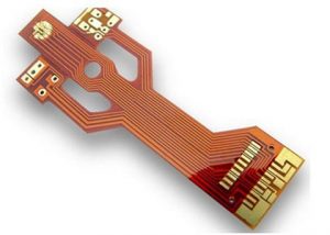
Vias Created During Flex PCB Fabrication
Vias are a critical component in the construction of flex PCBs. They connect the copper layers on the PCB with each other and are used to route signals through the board. In addition, vias are an important way to add mechanical support to a flexible circuit board. To ensure that the vias on a flex PCB are properly placed and function as intended, there is a process that must be followed during flex PCB fabrication.
The first step in the flex PCB fabrication process is designing the layout of the board using PCB design software. This allows for the proper placement of both rigid and flex components and traces. After the design is completed, output files are created that are then used for preparing the copper layers. In this phase, the layer thicknesses are set so that they are able to accommodate the expected electrical and mechanical requirements of the device. In addition, the correct impedance is maintained.
To create the necessary copper layers, a photochemical etching process is performed on the PCB material. The resulting copper is then printed on the flex PCB. After the copper is printed, small holes are drilled into the layers to connect them. These holes are then plated with copper to form solid and stable connections between the different layers. In order to prevent the solder from oxidizing or corroding these copper connections, it is necessary to apply a solder mask to the board.
How Are Vias Created During Flex PCB Fabrication?
During the flex PCB manufacturing process, it is crucial to use the right plating method for the circuit. Panel plating is a popular choice, but it can lead to stress concentration spots in the copper. In addition, it can increase the etch yield in intricate etched patterns. Alternatively, pad-only plating is preferred, as it allows manufacturers to control copper thickness and improves etch performance. Pad-only plating is more expensive, but it is essential for a quality flexible PCB.
Another key part of the flex pcb fabrication process is applying the required adhesives to the various layers. A polyimide film adhesive is typically utilized to attach the flexible sections of the circuit to the rigid areas. An adhesiveless option is also available, which uses a photoimageable solder mask to protect the copper traces.
In some cases, stiffeners are added to the flex PCB during fabrication. These are localized pieces of rigid material that can be attached to the flex circuit with acrylic thermally cured adhesives or pressure-sensitive adhesives. Stiffeners can help to reduce bending fatigue and increase abrasion resistance. They can also aid in weight balance and heat dissipation.
Finally, the finished flex PCB is tested for functionality and reliability. This testing can include visual inspection, electrical testing, and functional tests. These tests are vital to ensuring that the flex PCB is functioning as intended and is capable of enduring thousands of thermal cycles. Through ongoing innovations in back drilling, filling methods, and laser materials processing, vias are continuing to play a pivotal role in the development of cutting-edge PCBs that power everything from 5G wireless connectivity to advanced aircraft systems.