Component Damage During PCB Board Assembly
A porcelain bowl dropping on the ground may shattered with an obvious bang, but PCB boards are much more delicate and can suffer damage that isn’t as readily evident. Even so, a careful approach to PCB board assembly can minimize the risk of component damage. It starts with a carefully considered PCB layout and includes such things as adequate component spacing, proper trace routing, and impedance control.
Moisture sensitivity is another significant issue that can be minimized by following recommended moisture sensitivity guidelines. These include avoiding direct contact with ICs and other moisture-sensitive components and using appropriate packaging materials. Another precaution to take is using multiple vias at layer transitions, which helps reduce the sensitivity of high-current paths to moisture absorption and increases reliability.
The next major area of PCB layout that should be considered is the location and orientation of the power and ground planes, which can influence the assembly process and the performance of the circuit board in the final product. Ideally, both power and ground should be positioned on the same side of the PCB to simplify the assembly process. Additionally, it’s best to position the power and ground planes as close together as possible to ensure efficient current flow and to limit the number of copper-to-copper contacts that could lead to a short circuit during operation.
Minimizing the Risk of Component Damage During PCB Board Assembly
Other considerations during the PCB layout design phase include making sure that all plated through-hole (PTH) components are placed on one side of the board and that surface mount (SMT) components are placed on the other, which allows for more accurate alignment during assembly by pick-and-place machines. Also, be sure to provide independent pads for each component instead of having them share a pad; this can lead to tombstoning, a problem where one side of the component lifts away from the pad during reflow soldering.
Finally, be sure to provide heat sinks or dedicated copper planes for all power and ground-related components on the board to help prevent thermal stress and warping. This can be achieved by distributing heat-generating components evenly across the PCB or by incorporating an effective thermal relief pattern at the connection point of the pads and their respective copper planes.
While it’s impossible to eliminate all handling issues during pcb board assembly, these tips can greatly reduce the risk of damage to sensitive components and other problems that can negatively affect the quality and functionality of the final product. With the right PCB layout and the right PCB manufacturer, you can be confident that your product will deliver superior quality, durability, and reliability. After all, the last thing you want is to have to rework your prototype after it’s been delivered for manufacturing! For more information on optimizing your PCB layout, contact the PCB experts at AP Electronics today. We’ll be happy to answer any questions you have and help you get started with the best PCB manufacturing services for your project. We can’t wait to work with you!
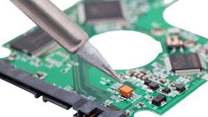
Utilize efficient soldering techniques such as surface mount technology (SMT) and reflow soldering. SMT allows for smaller components and higher component density, reducing PCB size and material costs.